1. Modifying your .cdsinit file
The .cdsinit file is an initialization file that runs when Cadence is starting. This section describes some useful additions to your .cdsinit file that you can add. The .cdsinit file is a hidden file and is often located in the directory where you start Cadence. This is not always the case and you may have to search for it. All these scripts can also be entered in the command line once cadence starts.
2. Changing the default text editor
When working with AHDL or VerilogA it is nice to have a choice of different text editors to use. To change the default text editor in Cadence, add the following to your .cdsinit file:
editor = "TEXT_EDITOR_NAME"
Where TEXT_EDITOR_NAME is an editor such as nedit, gedit, vim, ect. For a complete list of Linux text editors see: http://en.wikipedia.org/wiki/Category:Linux_text_editors
3. Close the "What's new" window
ddsNewsClose()
4. Resize the Command Interface Window (CIW)
hiResizeWindow(window(1) list(1:25 800:200))
The CIW is the command line window. The window size and position is set by defining the pixel positions of the bottom-left (BL) and top-right (TR) location of the window. The bottom-left corner of the screen is the origin. The syntax is
list([BL_horizontal_position]:[BL_vertical_position] [TR_horizontal_position]:[TR_vertical_position])
list(1:25 800:200) sets it up in the bottom left part of the screen.
5. Open the library manager window
ddsOpenLibManager()
6. Load bindkeys
Bindkeys are keyboard button definitions for commonly used functions. The following two commands set the bindkeys to those that are used by the AMS groups.
loadi "~cdsmgr/common/schBindKeys.il"
loadi "~cdsmgr/common/leBindKeys.il"
The first file is for schematic bindkeys and the second is for layout bind keys. If you would like to change the bindkeys, you can copy these files to your home directory, edit them, and load them by changing the path in the commands above.
If you would like to create your own bindkey, you must first know the SKILL function of the command you are trying to bind. If you don't know the SKILL function you can find it by having cadence print all input activity in the command window. In the ICFB command window select Options->Log Filter...->Show Input->menu commands. Now when you activate a command through a menu or the mouse, its SKILL function will be displayed in the command window. Just copy this function into your bindkeys file with the same syntax as the other bind keys.
Note : The above command does not work on Cadence 6 if your .cdsinit file contains the following:
let( (bindKeyFileList file path saveSkillPath)
bindKeyFileList = '(
"common_bindkeys.il" ; JTS, from Cadence
)
An easy fix if you have this script is to simply repalce the above with this:
let( (bindKeyFileList file path saveSkillPath)
bindKeyFileList = '(
"leBindKeys.il"
"schBindKeys.il"
)
Note 2: If you are using IBM processes, the "IBM_PDK" customization setup automatically adds the "IBM" Bindkeys. To replace them, just replace this path
loadi(strcat( ibmPdkPath "cms9flp/V1.5.0.0IBM/cdslib/Skill/ibmPdkBindkeys.il")))
with your path like this:
JonPath="/nfs/spectre/u9/guerberj/Cadence/90nm/IBM_90"
loadi(strcat( JonPath "leBindkeys.il")))
loadi(strcat( JonPath "schBindkeys.il")))
7. Changing the default simulation directory
envSetVal("asimenv.startup" "projectDir" 'string strcat("/scratch/" getShellEnvVar("USER")))
This sets the default simulation directory to /scratch/user_name where user_name is your login name. Adding the user name directory is a precaution so that other people will not over write your data. Storing data on scratch keeps your account space from filling up. Note that this is not backed up.
Another method would be to delete the default simulation directory for your process and replace it with a link to a scratch directory folder.
8. Set the undo limit to 10
hiSetUndoLimit(10)
9. Add a model files path
asiSetEnvOptionVal( asiGetTool('spectre) 'modelFiles '(("/model_file_path" "")) )
10. Unlock your files
Sometimes if your computer crashes or looses power while Cadence is open, many of your folders will have a file in them that ends in .cdslck. This file is created when you open a schematic for edit and prevents anyone from altering the file while you have it open. There are several ways to fix this problem:
Use the clsAdminTool
The path for this tool is: /nfs/guille/a2/rh80apps/cadence/current/tools/bin/clsAdminTool
Run clsAdminTool in a directory above your locked files.
Type ale . to list locked files below the current directory.
Type are . to unlock files below the current directory.
If you only had one or two windows open at the time of the crash, then just browse to the folder and delete the .cdslck file.
If you had many files open...
Open a terminal and type cd ~ to return to your home directory
Type find . -name "*.cdslck" This will find all the cdslck files.
If you want to delete all of these files type find . -name "*.cdslck" -exec rm -f {} \; This will delete all files containing .cdslock in the filename.
You can make people very mad at you if you run this command in a group directory
11. Cadence Segmentation Faults
One of the Most annoying things is when cadence crashes. Here are some things that will cause Cadence to crash:
In Virtuoso 6 do not hit the "Results > Print" Command while the simulation is running or else a crash is eminent
Monday, April 12, 2010
Wednesday, March 3, 2010
Short Range Wireless and Semiconductors
Bluetooth, NFC, UWB, 802.15.4 And Wi-Fi ICs Expected To Exceed Two Billion Units In 2010
March 1, 2010
Global shipments of short range wireless ICs (Bluetooth, NFC, UWB, 802.15.4, Wi-Fi) are expected to surpass two billion units this year, increasing approximately 20% compared to 2009. Shipments are forecast to total five billion in 2014, according to new market data from ABI Research.
"Bluetooth ICs made up a significant part of the total short range wireless ICs shipments," says industry analyst Celia Bo. "Bluetooth took more than 55%, following by Wi-Fi at around 35%; the rest of the shipments were made up of NFC, UWB and 802.15.4 ICs."
Mobile handsets maintain the highest adoption rate for Bluetooth ICs. In addition to data transmission between mobile handset and Bluetooth headset, the application of Bluetooth technology is gradually moving into computers and consumer electronics products such as laptops, UMDs, and the wireless remote pole of game consoles.
Low power consumption and short range transmission are two key technical features of Bluetooth technology. Furthermore, in December 2009 the Bluetooth Special Interest Group (SIG) announced the adoption of Bluetooth low energy (BLE) which opens an absolutely new market for products and devices needing low cost and low power wireless connectivity. Likely vertical markets include healthcare, security, and home entertainment.
Chip manufacturing technology migration is driving down chip cost too, and as Bluetooth chip ASPs continue to decline, new business opportunities will be created.
Combination chips, integrating two or more short range wireless technologies to deliver further cost reduction and chip size decreases, are paving the way for another trend in short range wireless IC market development. The three major integration solutions — Bluetooth+FM radio, Bluetooth+Wi-Fi+FM, and Bluetooth+FM+GPS — are forecast to account for more than 30% of all Bluetooth combination chip shipments in 2010. The combination chip using BLE is expected to make up 50% of total Bluetooth combo IC shipments in 2014.
ABI Research's "Short Range Wireless ICs Market Forecast Data" provides market and technical analysis of Bluetooth, NFC, UWB, 802.15.4, Wi-Fi and combination wireless connectivity ICs. The forecast information is broken down by application, including computers, communication devices and consumer electronic products.
The study is included in two of the firm's Research Services: Short Range Wireless and Semiconductors.
SOURCE: ABI Research
Wednesday, February 10, 2010
Calculation of inductance and Q from S parameter
For Single-ended inductor (equations valid in ADS):
L(f)=imag(1/y11)/(2*pi*f);
Q(f)=imag(1/y11)/real(1/y11);
For differential inductor:
Z=z11+z22-z12-z21;
L(f)=imag(Z)/(2*pi*f);
Q(f)=imag(Z)/real(Z);
L(f)=imag(1/y11)/(2*pi*f);
Q(f)=imag(1/y11)/real(1/y11);
For differential inductor:
Z=z11+z22-z12-z21;
L(f)=imag(Z)/(2*pi*f);
Q(f)=imag(Z)/real(Z);
Thursday, February 4, 2010
Update design library to a newer version for IBM 0.13um PDK
First, you need to update all the ENV setup files, .cdsinit, .cdsenv,…. and cds.lib files;
Second, you need to reissue the CDF callbacks. For update a whole library, you can do by invoking IBM_PDKàLibrary ibmPdk Parameter Check in CIW. For update one cell only, you can do by invoking IBM_PDKàCheckingàCDF parameter Check in cell view window. Remember you must save for both case.
For details, you may refer to the sections 1.2 and 6.2 of cmrf8sf.cdslib51.rel_notes.pdf
Wednesday, February 3, 2010
Difference between average power and RMS power
For digital circuits, the power consumption refers to average power.
RMS power is meaningless and misleading.
RMS is meaningful for Voltage and Current in a LINEAR circuits.
P=Vrms*Irms=Pave
For non-linear circuits, only average power should be calculated.
An analysis with simple examples can be found at:
http://www.eznec.com/Amateur/RMS_Power.pdf
RMS power is meaningless and misleading.
RMS is meaningful for Voltage and Current in a LINEAR circuits.
P=Vrms*Irms=Pave
For non-linear circuits, only average power should be calculated.
An analysis with simple examples can be found at:
http://www.eznec.com/Amateur/RMS_Power.pdf
Thursday, January 21, 2010
Figure of Merit (FoM) of LNA and Mixer
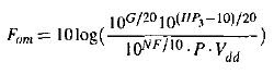
There are many different definitions of FoM for different LNAs (wideband LNA, low power LNA, etc.).
For low power LNA, one definition is [1]

Wherein, the Gain is power gain.
Another two definitions are [2]:


A Mixer's FoM can be defined as [3]:
References:
[1] LEE, H., MOHAMMADI, S. A 3GHz subthreshold CMOS low noise amplifier. In Radio Frequency Integrated Circuits (RFIC)
Symposium, 2006, p. 4.
[2] Linten, D.; Aspemyr, L.; Jeamsaksiri, W.; Ramos, J.; Mercha, A.; Jenei, S.; Thijs, S.; Garcia, R.; Jacobsson, H.; Wambacq, P.; Donnay, S.; Decoutere, S.;
VLSI Circuits, 2004. Digest of Technical Papers. 2004 Symposium on, 17-19 June 2004 Page(s):372 - 375
http://wwwtw.vub.ac.be/elec/Papers%20on%20web/Papers/DLinten/LintenVLSI2004.pdf
[3] Vidojkovic, V. Van der Tang, J. Leeuwenburgh, A. Van Roermund, A. Circuits and Systems, 2003. ISCAS '03. Proceedings of the 2003 International Symposium on, 25-28 May 2003, Volume: 2, On page(s): II-300- II-303 vol.2
For low power LNA, one definition is [1]

Another two definitions are [2]:


[1] LEE, H., MOHAMMADI, S. A 3GHz subthreshold CMOS low noise amplifier. In Radio Frequency Integrated Circuits (RFIC)
Symposium, 2006, p. 4.
[2] Linten, D.; Aspemyr, L.; Jeamsaksiri, W.; Ramos, J.; Mercha, A.; Jenei, S.; Thijs, S.; Garcia, R.; Jacobsson, H.; Wambacq, P.; Donnay, S.; Decoutere, S.;
VLSI Circuits, 2004. Digest of Technical Papers. 2004 Symposium on, 17-19 June 2004 Page(s):372 - 375
http://wwwtw.vub.ac.be/elec/Papers%20on%20web/Papers/DLinten/LintenVLSI2004.pdf
[3] Vidojkovic, V. Van der Tang, J. Leeuwenburgh, A. Van Roermund, A. Circuits and Systems, 2003. ISCAS '03. Proceedings of the 2003 International Symposium on, 25-28 May 2003, Volume: 2, On page(s): II-300- II-303 vol.2
Monday, January 4, 2010
Subscribe to:
Posts (Atom)
